
In case you find QProbe useful, you can get it. Either you build yourself from the attached files, or you order it.
Sadly in 2021 electronic components clearly increased in price. A kit is 140€, ready build and tested it is 220€.
Building
QProbe consists of these physical modules
- The main PCB, a quad-layer with gold fingers.
Best you order with SMD assembled.
The PCB can be produced by every maker via the given Gerber files.
The SMD assembly requires two special files for BOM (Bill Of Material) and positions, the attached ones are only suitable for the chinese maker JLCPCB. - the front panel template with LED holes. Its a PCB without copper layer, only color and drill holes, so it can be made together with the main PCB. Choose "black" color, 1.2mm tickness, and tell the manufacturer NOT to print his order numebr onto the board.
- The body for the 1.8mm LEDs. It is given as STL file and can be printed on every 3D printer. As it has fine details, the printer must have fairly high quality. I use a Prusa MK3S.
For the THT ("through-the-hole") components see the 2nd attached BOM.

Verifying PCB operation before main assembly:
PCB operation can be verify with this minimum procedure:
- Solder in capacitor C2 and C3 (to stabilize 3.3Volt), solder in sockets and plug in 180 ohm pull-up terminators RN32, RN34, RN36, RN38, RN40, RN42.
- populate the JTAG connector J2, and DIP switch SW1, set switch #1 to ON, all others OFF (LEDs show QBUS signals without additional logic).
- Apply +5V power to the legs of C2, verify C3 has 3.3 V. Temporarily insert (do not solder!) a 1.8mm LED at position D4 "+5V", cathode (short leg) toward the board edge. It should shine.
- you have 3.3V now, program the CPLD (see below).
- with all pull-up terminators installed, you can "assert" (activate) a QBUS signal by touching its pad on the breakout field with a GND wire (the pulldowns are optional in this step). The LED should shine. The schematic tells you LED labels and assigned signals. E.g.: DAL00 = ADDR00 is D6, DMR is D59.
CPLD programming
You need to program the two CPLDs. These are Intel (ex Altera) EPM240T100.
For programming you need
- work on a Win10 platform.
- buy a programming adapter: search on eBay for "altera usb blaster", it should be $5 to $10.
- install the "Intel Quartus Prime Lite Edition". This is quite a big pack, also stand-alone programmers are available.
- After installing Quartus, plug in USBBlaster and install its driver, which is well hidden inside the Quartus file tree.
For me it was "c:\intelFPGA_lite\20.1\quartus\drivers\usb-blaster-ii\". - Then power the QPRobe board with +5V, plug USBBlaster onto the JTAG header, start Quartus, go to the Tools/Programmer menu, select your USBBlaster as hardware, "Detect" both CPLDs, and load each of the both *pof" file into its matching CPLD.
Workflow in Quartus-Programmer's GUI for CPLD1, before repeating for CPLD2:

Component assembly
There's not much to say for the soldering part. Just several 100s pins ...
LED assembly
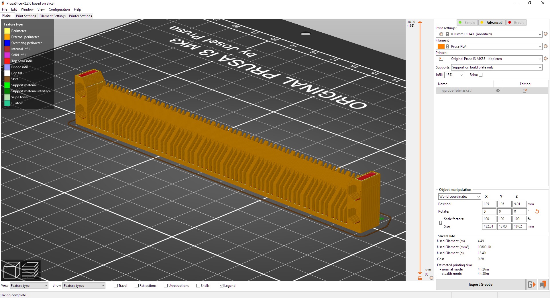
I printed the LED body on an Prusa MK3S in out-of-the-box configuration (mid of 2020).
Filament was the one delivered with the printer, "PLA Silver made for Prusa Research", Prusa's order number FLM-PLA-175-SLV.
Printing quality was "0.10mm DETAIL". The only special setting was a larger "Print Settings/Support material/Contact Z distance" of 0.2 instead of 0.1, to allow easier remove of struts.
Attached is a screenshot of PrusaSlicer.
It's important to print the STL rotated, with LED openings down to the headbed. This way pin holes remain open, and you have minimal struts to remove.

LED orientation
To make the orientation fool-proof: The anode pin of a LED is on the ROUND side of the LED body, and when looking onto the front goes to the LEFT.
The cathode pin is on the SQUARE side and goes to the RIGHT.

 |
 |
If you like to test the LEDs (china stuff?) before mounting: apply +5V to the QProbe, and use the "+5V" LED position as test adapter.
LED mount
Mounting the LEDs into the body onto the PCB is the hard part, at least laborious. (Don't blame me, you wanted to build the kit!)
Best proceed in these steps:
- Open the pin holes in the 3D body with a 1mm drill. Press the nuts into the LED print and test-mount with 4 screws, then unscrew.
- Clean the LED holes in the 3D print.
- Test insert all LEDs, you may have to push them into the 3D print with some force.
- The front panel PCB is just snapped onto the 60 LEDs. It will need rework, open the LED holes with a 2mm drill.
- Repeat 2-4 until the front panel fits correctly.
- Insert only the lower LED row (IAK..+12V) in to the LED body.
- Bend the LED pins in a 90° degree, but with 2.5 mm distance to the LED body's edge!
- Fiddle all the LED pins into the PCB. You'll need some tool to keep the PCB and LED body in place.
I used my Prusa-Printer to move the LEDs toward the PCB in controlled way:
Here the LED body is tied to the x-Axis slightly rotated (black helper adapter). Then the x-Axis is moved slowly downward under manual control, you can insert the LED pins one-by-one into the PCB then. - Finally screw the LED body to the PCB again. Sort out the bended LED pins, then you can do a first function test before soldering (see below).
- Solder the lower LED row.
- Insert LEDs into the upper row. Best pre-bend the pins into a wide 180° arc, then "roll" them through the 3D body into their pin holes.

Verify
To finally verify your build again, plug in at least pullup bus termination resistor packs, apply +5V power to the board and set the CPLD mode switches #1 and #2 to ON (LED shows bussignals directly, and "DATA is a copy of ADDRESS"). Then touch each QBUS signal pin with a GND wire to assert them one-by-one (QBUS signals are inverted: a logic 1 is presented by 0 volt signal level). Verify the selected LEDs are shining. For BDAL<15:0>, both an ADDR and a DATA LED are active together if switch #2 is ON.
When you set all DIP switches to the OFF position, you have additional LED logic. For IRQ, UIAK, DMR,DMG and SACK this means: short pulses are elongated to 100ms. So if scatching these siangal pins with your GND wire, you should see no flicker anymore but a steady light.
qprobe.zip -- Gerber files for main PCB
qprobe-top-pos.csv -- SMD positions JLCPCB. \"CPL\" = \"Component Placement List\"
qprobe-front.zip -- Gerber files for LED front panel
qprobe-ledbody.stl -- LED body 3D print
QProbe-lowerleds-bender.stl -- Helper to bend lower LED pins 3D print
schematic.pdf -- QProbe schematic
qprobe-bom_jlcpcb.csv -- SMD Bill Of Material for JLCPCB
QProbeCPLD1.pof -- Binary pattern for CPLD1
QProbeCPLD2.pof -- Binary pattern for CPLD2
qprobe-ledbody-prusaslicer.jpg -- LED body 3D print PrusaSlicer screenshot